
PCB Prototyping Services
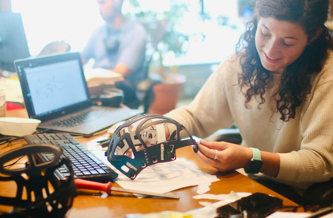
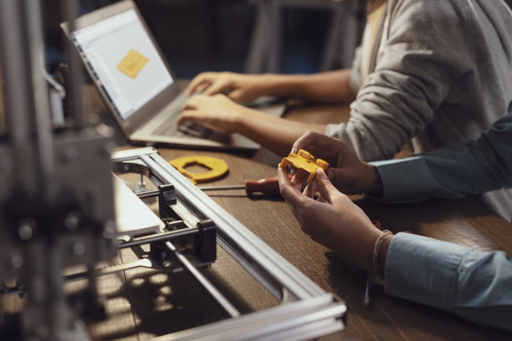
At CircuitEDGE, we provide fast, reliable PCB prototyping services tailored for R&D teams, hardware startups, and engineering organizations that require accuracy, repeatability, and manufacturability from the very first build. Our prototyping process is engineered to support design validation, functional testing, and iterative development, ensuring a smooth transition from prototype to volume production.
Engineering-Driven Prototyping
PCB prototyping is not just about quick turnaround—it is about building the right board, the right way. CircuitEDGE works closely with design engineers to ensure prototypes meet electrical, mechanical, and manufacturing requirements.
Our focus areas include:
1. Signal integrity and power integrity readiness
2. Stack-up optimization and controlled impedance
3. DFM / DFA feedback before fabrication
4. Material selection aligned with final production goals
Typical Use Cases
Our PCB prototyping services are commonly engaged at critical development stages where performance validation, design accuracy, and rapid iteration are essential.
1. Product R&D and feasibility studies
2. Hardware validation and design iterations
3. Proof-of-concept (PoC) builds
4. RF, high-speed digital, and mixed-signal designs
5. Pre-certification and compliance testing builds
Each use case is supported with production-aware engineering to ensure a smooth path from prototype validation to scalable manufacturing.
Prototyping Capabilities
A. PCB Technology
1. Single-layer to multilayer PCBs (up to high-density designs)
2. FR-4, High-Tg FR-4, Rogers, and other RF/High-speed laminates
3. HDI prototyping: microvias, blind/buried vias
4. Controlled impedance traces
5. Fine-pitch BGA, QFN, and LGA compatible layouts
B. Fabrication Parameters
1. Minimum trace/space: as per advanced prototype standards
2. Small via and microvia structures
3. Tight tolerance stack-ups
4. Lead-free, RoHS-compliant processes
C. Assembly (PCBA Prototyping)
1. SMT and THT assembly
2. Fine-pitch and BGA assembly
3. Mixed-technology boards
4. Low-volume, high-mix builds
5. Component sourcing support
D. Prototype to Production Continuity
Many R&D projects fail during scale-up due to poor prototype decisions. CircuitEDGE prototypes are production-aware by design, minimizing redesign risks and cost escalations later.
We ensure:
1. BOM optimization for availability and lifecycle
2. Panelization considerations for volume runs
3. Assembly yield optimization
4. Test-point planning for future ICT/FCT
E. Quality & Verification
Every prototype undergoes strict quality checks aligned with IPC standards:
1. Electrical testing (netlist-based)
2. AOI for assembled boards
3. Visual and dimensional inspection
4. Optional functional testing support
- Discover how our expertise can help with your next PCB project.