
Component Supply Chain
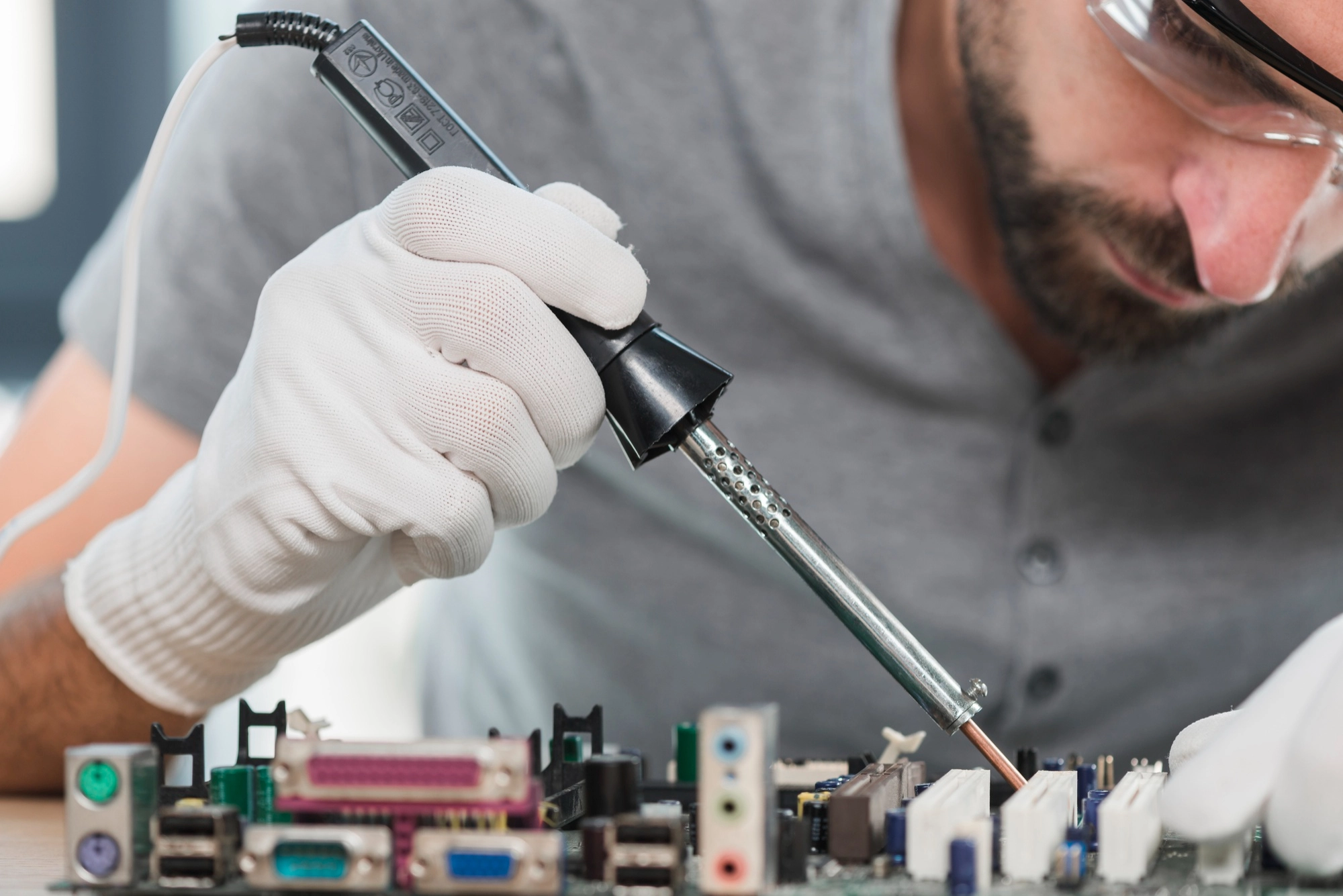
Reliable component sourcing is critical to the success of any electronic product. At CircuitEDGE, our Components Supply capability is designed to support stable production, mitigate supply-chain risk, and ensure component authenticity across the entire PCB and PCBA lifecycle.
Global Component Sourcing with Engineering Oversight
CircuitEDGE sources electronic components through a vetted global supplier network, including authorized distributors, OEM channels, and approved supply partners. Every sourcing decision is guided by engineering requirements, lifecycle considerations, and availability constraints.
Our sourcing scope includes:
1. Active components (MCUs, FPGAs, processors, power devices)
2. Passive components (resistors, capacitors, inductors)
3. Electromechanical parts (connectors, relays, switches)
4. RF, high-speed, and power electronics components
All components supplied are new, original, and traceable.

Supply Chain Risk Management
Component shortages, obsolescence, and price volatility are common challenges in today’s electronics market. CircuitEDGE proactively manages these risks by:
1. Monitoring availability and lead times
2. Identifying qualified alternative components
3. Supporting form-fit-function (FFF) substitutions
4. Aligning sourcing strategy with product lifecycle requirements
This approach helps maintain production continuity without compromising performance or reliability.
High Density Interconnect (HDI)
As printed circuit board (PCB) form factors decrease and functionality increases, the result is a dense packaging challenge that often must incorporate blind and buried vias, laser microvias, via-in-pad and complex stackups. The potential for electromagnetic interference (EMI) to impact design performance is high.
AdvancedPCB’s experienced designers, which have a strong working knowledge of EMI principles, work closely with product engineers to ensure that packaging complexity does not translate into issues in signal or power integrity. This approach to PCB solvability and a focus on electrical integrity and end product manufacturability help ensure a workable layout on the first spin. Key elements contributing to efficient HDI layout includes:
- The team’s ability to match the right tools with the right designers for specific product requirements.
- A commitment to continuous learning that helps ensure the design team is familiar with the latest industry-standard best practices and design rules.
- A collaborative, gated approach that aligns resources with the product development timetable to ensure a working layout is delivered on time and on budget.
- Designers with a robust working knowledge of stackups and utilization of via technology to realize complex routing topologies.
| Items | Capabilities |
|---|---|
| Max Layer | 16L |
| Inner Layer Min Trace/Space | 3/3mil |
| Out Layer Min Trace/Space | 3.5/4mil |
| Out Layer Min Trace/Space | 2oz |
| Inner Layer Max Copper | 2oz |
| Out Layer Max Copper | 0.1mm |
| Min Mechanical Drilling | 0.1mm |
| Min Laser Drilling | 0.1mm |
| Aspect Ratio(Mechanical Drilling) | 10:1 |
| Aspect Ratio(Laser Drilling) | / |
| Press Fit Hole Tolerance | ±0.05mm |
| PTH Tolerance | ±0.075mm |
| NPTH Tolerance | ±0.05mm |
| Countersink Tolerance | ±0.15mm |
| Board Thickness | 0.1-0.5mm |
| Board Thickness Tolerance(<1.0mm) | ±0.05mm |
| Board Thickness Tolerance(≥1.0mm) | / |
| Impedance Tolerance | Differential:±5Ω(≤50Ω),±10%(>50Ω) |
| Single-Ended:±5Ω(≤50Ω),±10%(>50Ω) | |
| Min Board Size | 5*10mm |
| Max Board Size | 9*14inch |
| Contour Tolerance | ±0.05mm |
| Min BGA | 7mil |
| Min SMT | 7*10mil |
| Surface Treatment | ENIG,Gold Finger,Immersion Silver,Immersion |
| Tin,HASL,OSP,ENEPIG,Flash Gold;Hard gold plating | |
| Solder Mask | Green Solder Mask/Black PI/Yellow PI |
| Min Solder Mask Clearance | 3mil |
| Min Solder Mask Dam | 8mil |
| Legend | White,Black,Red,Yellow |
| Min Legend Width/Height | 4/23mil |
| Strain Fillet Width | 1.5±0.5mm |
| Bow & Twist | / |
- Discover how our expertise can help with your next PCB project.