
PCB Design Services
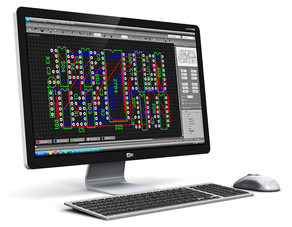
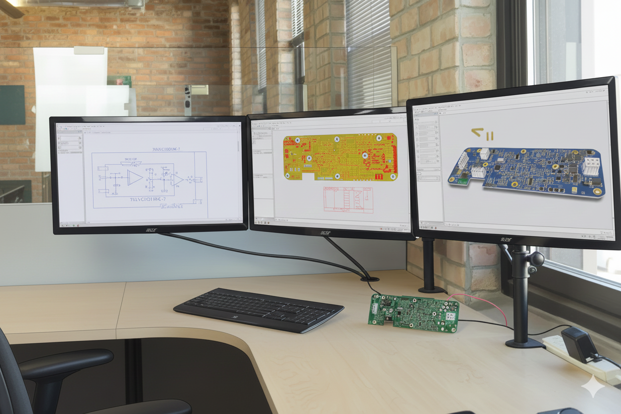
CircuitEDGE delivers end-to-end PCB design services engineered for performance, reliability, and manufacturability. Our design capabilities span schematic capture, PCB layout, stack-up planning, controlled-impedance routing, and high-speed/RF design, ensuring optimal electrical behavior from concept to production. Using industry-leading EDA tools, we produce accurate manufacturing and assembly documentation, ensuring seamless transition from design to fabrication, testing, and volume production—resulting in high-performance, fully manufacturable, and test-ready PCBs.
End-to-End PCB Design Services
Modern electronic products demand PCB designs that balance performance, reliability, and manufacturability—often under tight timelines and complex technical constraints. CircuitEDGE offers comprehensive PCB design services that help organizations move confidently from concept to production without costly redesigns or delays.
We support customers across aerospace, automotive, defense, telecommunications, industrial automation, medical, energy, cloud computing, and consumer electronics, providing design solutions tailored to each industry’s technical and regulatory requirements. Whether supporting early-stage prototyping or production-ready designs, our engineers bridge the gap between electrical design intent and real-world manufacturing.
Our PCB design services cover the complete development lifecycle, including schematic capture, stack-up definition, component selection, high-density PCB layout, and controlled-impedance routing. We integrate DRC, DFM, DFA, and DFT best practices early in the process to ensure designs are optimized for fabrication, assembly, and testing from the outset.
PCB Design Capabilities
We support projects from early schematic capture to final Gerber release, covering low-speed digital to high-speed, RF, power, and mixed-signal designs.
1. Schematic Design & Review
2. Multilayer PCB Layout
3. High-Speed Digital Design
4. RF & Microwave PCB Design
5. Power Electronics & Analog Design
6. Simulation, Verification & Compliance
Whether you need a fresh design, design optimization, or a second-opinion review, CircuitEDGE is your trusted PCB design partner.
Contact us to discuss your technical requirements.
High Density Interconnect (HDI)
As printed circuit board (PCB) form factors decrease and functionality increases, the result is a dense packaging challenge that often must incorporate blind and buried vias, laser microvias, via-in-pad and complex stackups. The potential for electromagnetic interference (EMI) to impact design performance is high.
AdvancedPCB’s experienced designers, which have a strong working knowledge of EMI principles, work closely with product engineers to ensure that packaging complexity does not translate into issues in signal or power integrity. This approach to PCB solvability and a focus on electrical integrity and end product manufacturability help ensure a workable layout on the first spin. Key elements contributing to efficient HDI layout includes:
- The team’s ability to match the right tools with the right designers for specific product requirements.
- A commitment to continuous learning that helps ensure the design team is familiar with the latest industry-standard best practices and design rules.
- A collaborative, gated approach that aligns resources with the product development timetable to ensure a working layout is delivered on time and on budget.
- Designers with a robust working knowledge of stackups and utilization of via technology to realize complex routing topologies.
| Items | Capabilities |
|---|---|
| Max Layer | 16L |
| Inner Layer Min Trace/Space | 3/3mil |
| Out Layer Min Trace/Space | 3.5/4mil |
| Out Layer Min Trace/Space | 2oz |
| Inner Layer Max Copper | 2oz |
| Out Layer Max Copper | 0.1mm |
| Min Mechanical Drilling | 0.1mm |
| Min Laser Drilling | 0.1mm |
| Aspect Ratio(Mechanical Drilling) | 10:1 |
| Aspect Ratio(Laser Drilling) | / |
| Press Fit Hole Tolerance | ±0.05mm |
| PTH Tolerance | ±0.075mm |
| NPTH Tolerance | ±0.05mm |
| Countersink Tolerance | ±0.15mm |
| Board Thickness | 0.1-0.5mm |
| Board Thickness Tolerance(<1.0mm) | ±0.05mm |
| Board Thickness Tolerance(≥1.0mm) | / |
| Impedance Tolerance | Differential:±5Ω(≤50Ω),±10%(>50Ω) |
| Single-Ended:±5Ω(≤50Ω),±10%(>50Ω) | |
| Min Board Size | 5*10mm |
| Max Board Size | 9*14inch |
| Contour Tolerance | ±0.05mm |
| Min BGA | 7mil |
| Min SMT | 7*10mil |
| Surface Treatment | ENIG,Gold Finger,Immersion Silver,Immersion |
| Tin,HASL,OSP,ENEPIG,Flash Gold;Hard gold plating | |
| Solder Mask | Green Solder Mask/Black PI/Yellow PI |
| Min Solder Mask Clearance | 3mil |
| Min Solder Mask Dam | 8mil |
| Legend | White,Black,Red,Yellow |
| Min Legend Width/Height | 4/23mil |
| Strain Fillet Width | 1.5±0.5mm |
| Bow & Twist | / |
- Discover how our expertise can help with your next PCB project.