
As electronic systems continue to push higher data rates, tighter tolerances, and greater functional density, PCB design has become a primary determinant of system performance and reliability. Signal integrity issues are rarely caused by a single factor; instead, they emerge from a series of design decisions made early in the PCB layout and stack-up planning stages.
Understanding how layout, materials, impedance control, and power distribution interact is essential for building reliable, high-performance electronics.
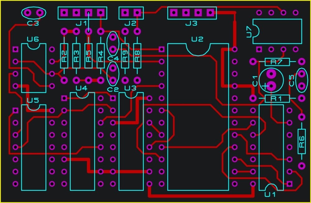
Layout Decisions and Signal Integrity
PCB layout directly affects how signals propagate across the board. Trace length, routing topology, spacing, and reference plane continuity all influence signal quality. Poorly routed high-speed traces can introduce reflections, crosstalk, and timing skew, leading to intermittent failures that are difficult to diagnose in later stages.
Key layout considerations include:
- Maintaining continuous reference planes for return current paths
- Avoiding unnecessary stubs and vias on high-speed signals
- Controlling trace spacing to minimize crosstalk
- Matching trace lengths for differential and timing-critical signals
Even small layout compromises can degrade eye diagrams, increase bit error rates, or reduce noise margins in real-world operation.
Stack-Up Planning and Material Selection
PCB stack-up design is foundational to signal integrity. Layer count, dielectric thickness, copper weight, and material selection determine impedance behavior and signal attenuation.
High-speed and high-frequency designs often require:
- Controlled dielectric thickness for impedance stability
- Low-loss materials to reduce signal attenuation
- Dedicated ground and power planes to stabilize reference paths
Selecting the wrong material or stack-up configuration can limit system bandwidth, increase EMI susceptibility, and reduce overall reliability.
Impedance Control and Power Integrity
Controlled impedance routing is no longer optional for modern electronics. Interfaces such as DDR, PCIe, Ethernet, USB, and high-speed serial links demand precise impedance matching to prevent reflections and signal distortion.
Equally important is power integrity. Inadequate decoupling, poor plane segmentation, or excessive via inductance can cause voltage droop and noise, directly impacting signal quality and long-term component reliability.
Real-World Performance and Reliability
Signal integrity issues often appear under temperature variation, vibration, or extended operating hours—conditions that laboratory testing may not fully replicate. Designs optimized for manufacturability, thermal stability, and electrical robustness perform more consistently over time.
At CircuitEDGE, PCB design is approached as a system-level discipline—balancing electrical performance, manufacturability, and reliability from the earliest design stages.
Conclusion
Every PCB design decision carries long-term consequences. Thoughtful layout, well-planned stack-ups, controlled impedance, and strong power integrity practices are essential to building reliable electronic systems that perform as intended in real-world environments.
Signal integrity is not a post-layout fix—it is engineered from the ground up.sectetur.