
IPC-6012 / IPC-A-610 Class 2 or Class 3

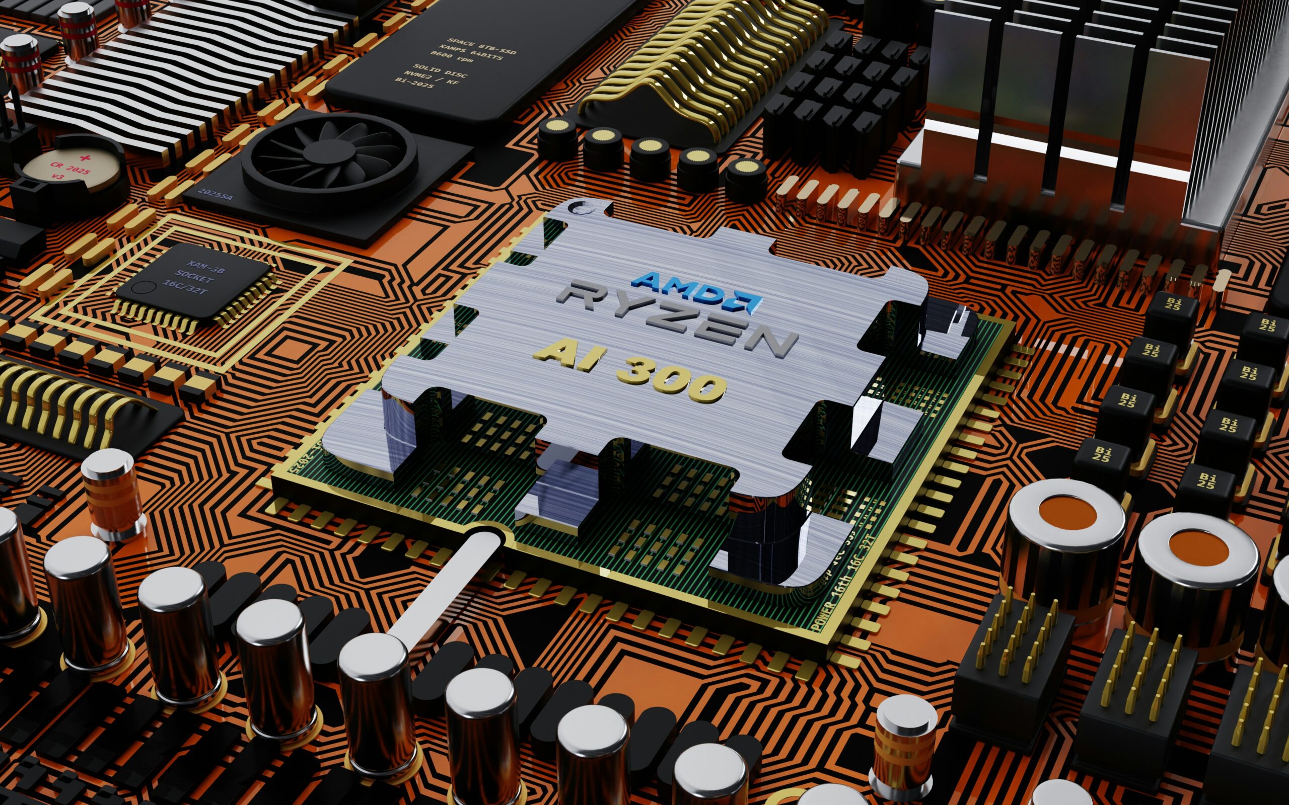
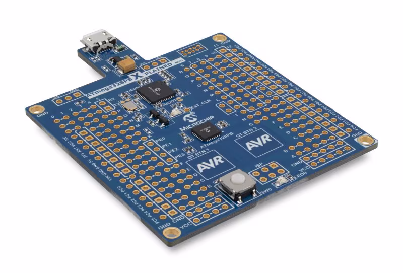
Chip Evaluation & Development Boards
CircuitEDGE manufactures PCBs for ASIC, FPGA, microcontroller, RFIC, and mixed-signal chip evaluation platforms. These boards prioritize stable impedance, clean signal paths, and precise interconnects for accurate device characterization
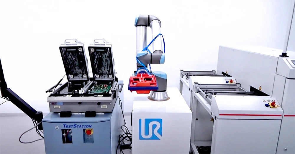
Automated Test Equipment (ATE) & Test Fixtures
We build high-density PCBs used in semiconductor testing environments, including probe card interfaces, load boards, interface boards, and instrumentation PCBs. Tight tolerances and low-loss materials ensure reliable measurement accuracy.

Power Semiconductor Drivers & Control Units
Our boards support Si, SiC, and GaN semiconductor drivers used in power modules, converters, motor control, and high-efficiency switching systems. Designs feature reinforced isolation, thermal optimization, and robust creepage/clearance.
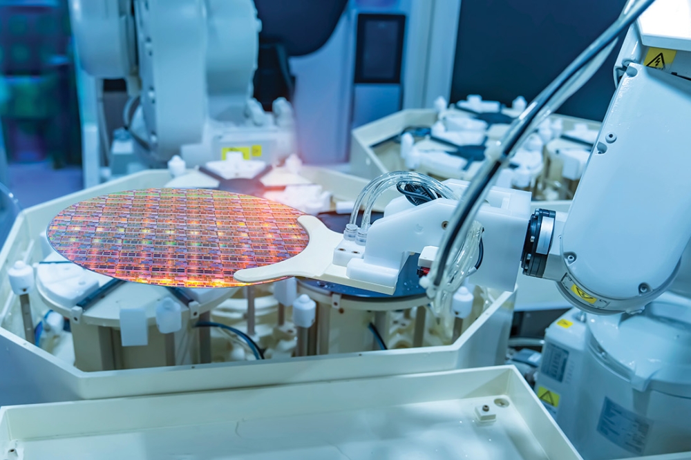
Semiconductor Manufacturing Equipment Electronics
CircuitEDGE produces PCBs for wafer handling systems, lithography modules, deposition equipment, plasma tools, and automated inspection devices. Reliability, temperature stability, and EMI robustness are priorities for these systems.
High-Speed Digital Platforms
We manufacture high-density boards for multi-gigabit SerDes, DDR interfaces, PCIe modules, high-bandwidth memory controllers, and other semiconductor-related digital platforms.

RF & Microwave Semiconductor Systems
Boards for RFIC characterization, mmWave verification, low-noise amplifiers, phased-array modules, and transceiver development use advanced laminates and RF-optimized routing strategies.