
As electronic products continue to shrink while performance requirements increase, fine-pitch and high-density PCB assemblies have become the norm rather than the exception. Packages such as BGAs, QFNs, CSPs, and ultra-fine-pitch components introduce assembly challenges that demand precise process control, disciplined inspection, and reliability-driven decision making.
Assembly success in these designs is determined long before the first component is placed.
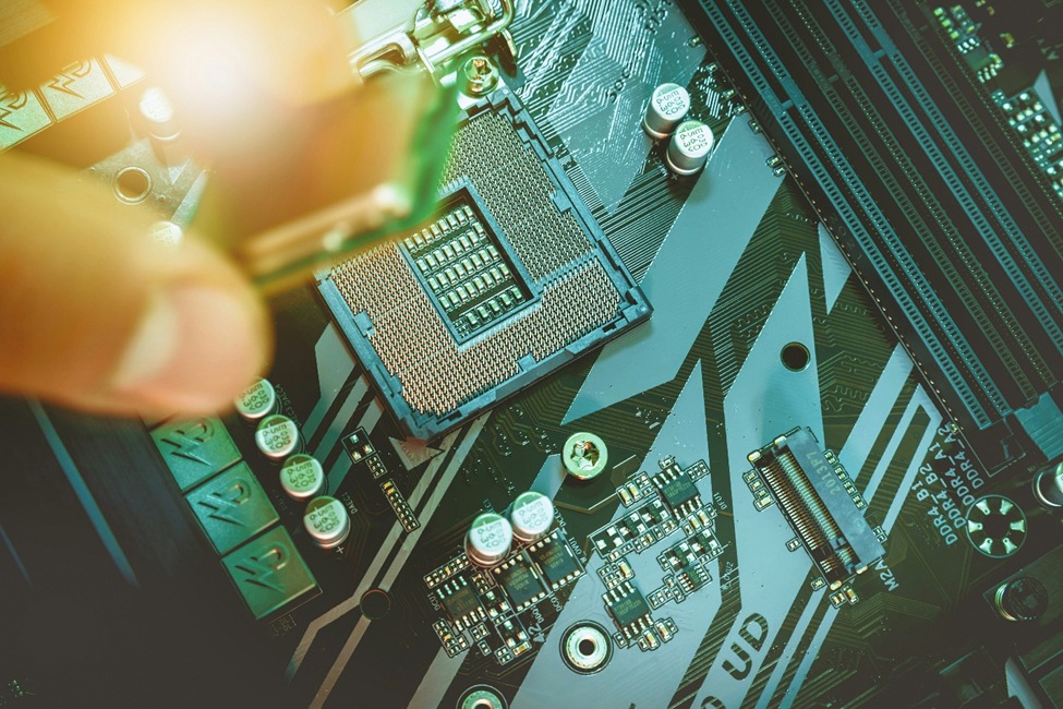
Key SMT Challenges in High-Density Assemblies
Fine-pitch designs significantly reduce margin for error. Small variations in solder volume, placement accuracy, or thermal profiles can result in defects such as bridging, tombstoning, voiding, or insufficient solder joints.
Common assembly challenges include:
- Fine-pitch lead spacing and tight pad geometries
- High component density limiting rework access
- BGA and QFN packages with hidden solder joints
- Mixed package sizes on a single PCB
- Thermal imbalance across densely populated areas
Addressing these challenges requires alignment between PCB design, stencil strategy, and placement accuracy.
Stencil Design and Solder Paste Control
Stencil thickness, aperture design, and solder paste selection directly affect joint quality. Fine-pitch components often require stepped stencils, reduced apertures, or modified shapes to control solder volume and prevent bridging.
Equally important is solder paste handling. Paste age, storage conditions, and print consistency must be tightly controlled to avoid defects that only appear under thermal cycling or long-term operation.
Reflow Profiling and Thermal Management
High-density assemblies frequently contain components with different thermal sensitivities. A poorly optimized reflow profile can stress components, damage laminates, or create latent reliability failures.
Best practices include:
- Profile optimization based on actual board mass and copper distribution
- Controlled ramp rates to reduce component stress
- Balanced peak temperatures across dense layouts
Thermal consistency is essential for long-term reliability.
Inspection Strategies for Fine-Pitch Assemblies
Visual inspection alone is insufficient for modern high-density PCBs. Automated Optical Inspection (AOI) identifies placement and solder issues on visible joints, while X-ray inspection is essential for BGAs, QFNs, and hidden connections.
Effective inspection strategies combine:
- AOI for surface-level defects
- X-ray for hidden solder joints and void analysis
- Targeted manual inspection for critical areas
Inspection data should feed back into process optimization rather than serving only as a pass/fail gate.
Reliability Considerations
Fine-pitch assemblies are more sensitive to mechanical stress, thermal cycling, and vibration. Design and assembly decisions should consider long-term reliability, not just initial yield.
Factors impacting reliability include:
- Pad geometry and solder joint shape
- PCB warpage control
- Component placement symmetry
- Stress relief through layout and stack-up design
Conclusion
Successful fine-pitch and high-density PCB assembly is the result of engineering discipline, process control, and inspection strategy working together. When design intent, assembly execution, and quality validation are aligned, even the most complex assemblies can be produced reliably and at scale.
At CircuitEDGE, PCB assembly is approached as an engineering process—ensuring complex designs are not only buildable, but dependable throughout their lifecycle.