
PCB Assembly Services
CircuitEDGE provides comprehensive PCB assembly services supporting prototype builds, pilot runs, and low- to mid-volume production. Our assembly processes are engineered for accuracy, repeatability, and reliability—ensuring each assembled board meets the electrical, mechanical, and quality requirements of its intended application.
PCB Assembly
CircuitEDGE supports customers across Dubai, United Arab Emirates, the GCC, and global markets through a controlled assembly ecosystem aligned with international quality standards. We assemble PCBs for applications spanning aerospace, automotive, defense, telecommunications, industrial automation, medical, energy, cloud computing, and consumer electronics.
Each assembly project begins with a detailed assembly feasibility and BOM review to ensure component compatibility, footprint accuracy, and process readiness before production begins.
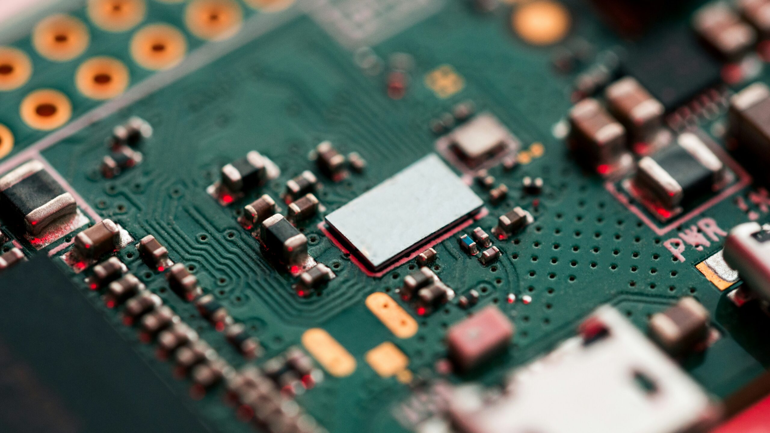

PCB Assembly Capabilities
CircuitEDGE supports a wide range of PCB assembly technologies, including:
• Surface Mount Technology (SMT) assembly
• Through-Hole Technology (THT) assembly
• Mixed-technology assembly
• Fine-pitch and ultra-fine-pitch components
• BGA, QFN, LGA, CSP, and PoP packages
• Double-sided and multilayer assemblies
• High-density and HDI board assemblies
Assembly processes are selected and optimized based on component types, board complexity, and reliability requirements.
Assembly Engineering & Process Control
Assembly quality is driven by preparation and process control. CircuitEDGE applies a structured engineering workflow that includes:
- BOM verification and component cross-checking
- Footprint and land-pattern validation
- Stencil design and solder paste selection
- Placement accuracy optimization
- Reflow profile development and validation
- Thermal stress control for sensitive components
| Items | Capabilities |
|---|---|
| Max Layer | 16L |
| Inner Layer Min Trace/Space | 3/3mil |
| Out Layer Min Trace/Space | 3.5/4mil |
| Out Layer Min Trace/Space | 2oz |
| Inner Layer Max Copper | 2oz |
| Out Layer Max Copper | 0.1mm |
| Min Mechanical Drilling | 0.1mm |
| Min Laser Drilling | 0.1mm |
| Aspect Ratio(Mechanical Drilling) | 10:1 |
| Aspect Ratio(Laser Drilling) | / |
| Press Fit Hole Tolerance | ±0.05mm |
| PTH Tolerance | ±0.075mm |
| NPTH Tolerance | ±0.05mm |
| Countersink Tolerance | ±0.15mm |
| Board Thickness | 0.1-0.5mm |
| Board Thickness Tolerance(<1.0mm) | ±0.05mm |
| Board Thickness Tolerance(≥1.0mm) | / |
| Impedance Tolerance | Differential:±5Ω(≤50Ω),±10%(>50Ω) |
| Single-Ended:±5Ω(≤50Ω),±10%(>50Ω) | |
| Min Board Size | 5*10mm |
| Max Board Size | 9*14inch |
| Contour Tolerance | ±0.05mm |
| Min BGA | 7mil |
| Min SMT | 7*10mil |
| Surface Treatment | ENIG,Gold Finger,Immersion Silver,Immersion |
| Tin,HASL,OSP,ENEPIG,Flash Gold;Hard gold plating | |
| Solder Mask | Green Solder Mask/Black PI/Yellow PI |
| Min Solder Mask Clearance | 3mil |
| Min Solder Mask Dam | 8mil |
| Legend | White,Black,Red,Yellow |
| Min Legend Width/Height | 4/23mil |
| Strain Fillet Width | 1.5±0.5mm |
| Bow & Twist | / |
- Discover how our expertise can help with your next PCB project.