
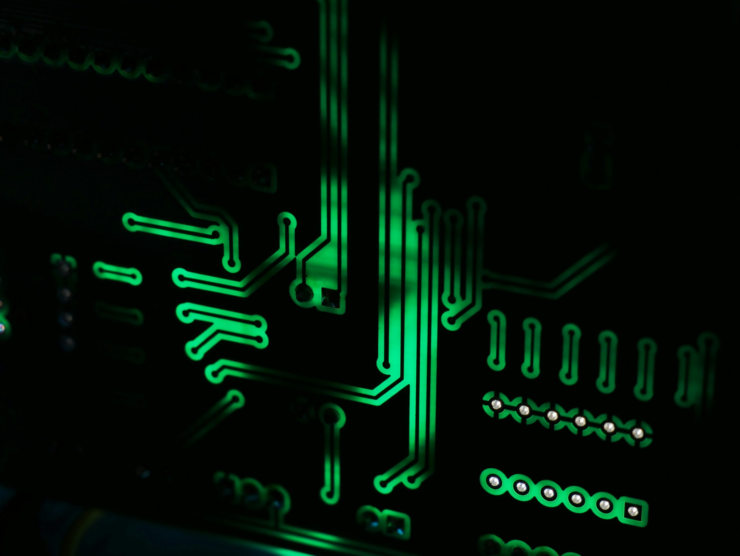
PCB Fabrication Capabilities
CircuitEDGE provides advanced PCB fabrication services engineered to support the full product lifecycle—from early-stage prototypes to volume production. Our fabrication capabilities span multilayer PCBs, HDI constructions, heavy-copper boards, and high-frequency designs, enabling reliable performance across a wide range of technical requirements.
PCB Fabrication and Manufacturing
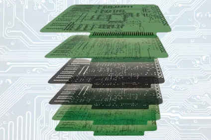
CircuitEDGE delivers comprehensive PCB fabrication solutions supporting both standard and advanced board technologies. Our capabilities include multilayer PCB fabrication, HDI structures, flexible PCBs, and rigid-flex constructions, enabling reliable solutions for a wide range of electronic applications.
Through controlled, ISO-aligned manufacturing processes and advanced fabrication equipment, we ensure high dimensional accuracy, electrical performance, and repeatability across every build. We support customers across medical, aerospace, automotive, telecommunications, industrial automation, energy, and consumer electronics, offering flexible fabrication models for rapid prototypes, cost-optimized production, and custom manufacturing at scale.
By working with CircuitEDGE, customers gain a fabrication partner focused on engineering precision, predictable lead times, and production consistency. Our fabrication workflows are designed to transition designs smoothly from prototype to volume manufacturing—delivering PCBs that meet technical requirements while maintaining cost efficiency and long-term reliability.
PCB Fabrication Capabilities
CircuitEDGE offers a wide range of PCB fabrication technologies, including:
• Single-sided, double-sided, and multilayer PCBs
• High-Density Interconnect (HDI) PCBs with microvias, blind and buried vias
• High-speed digital PCBs with controlled impedance stackups
• RF and microwave PCBs using low-loss materials
• Heavy-copper PCBs for power and high-current applications
• Flexible and rigid-flex PCBs
• High-temperature and high-reliability PCB constructions
Fabrication parameters are selected based on electrical, mechanical, thermal, and environmental performance requirements.
Materials & Stackup Engineering
Material selection is a critical part of PCB fabrication. CircuitEDGE supports a wide range of laminates and prepregs, including:
• Standard and high-TG FR-4
• Low-loss and high-speed digital materials
• RF and microwave substrates
• Polyimide and high-temperature materials
• Halogen-free and environmentally compliant materials
Stackups are engineered to achieve impedance targets, signal integrity, thermal stability, and manufacturability.
| Items | Capabilities |
|---|---|
| Max Layer | 16L |
| Inner Layer Min Trace/Space | 3/3mil |
| Out Layer Min Trace/Space | 3.5/4mil |
| Out Layer Min Trace/Space | 2oz |
| Inner Layer Max Copper | 2oz |
| Out Layer Max Copper | 0.1mm |
| Min Mechanical Drilling | 0.1mm |
| Min Laser Drilling | 0.1mm |
| Aspect Ratio(Mechanical Drilling) | 10:1 |
| Aspect Ratio(Laser Drilling) | / |
| Press Fit Hole Tolerance | ±0.05mm |
| PTH Tolerance | ±0.075mm |
| NPTH Tolerance | ±0.05mm |
| Countersink Tolerance | ±0.15mm |
| Board Thickness | 0.1-0.5mm |
| Board Thickness Tolerance(<1.0mm) | ±0.05mm |
| Board Thickness Tolerance(≥1.0mm) | / |
| Impedance Tolerance | Differential:±5Ω(≤50Ω),±10%(>50Ω) |
| Single-Ended:±5Ω(≤50Ω),±10%(>50Ω) | |
| Min Board Size | 5*10mm |
| Max Board Size | 9*14inch |
| Contour Tolerance | ±0.05mm |
| Min BGA | 7mil |
| Min SMT | 7*10mil |
| Surface Treatment | ENIG,Gold Finger,Immersion Silver,Immersion |
| Tin,HASL,OSP,ENEPIG,Flash Gold;Hard gold plating | |
| Solder Mask | Green Solder Mask/Black PI/Yellow PI |
| Min Solder Mask Clearance | 3mil |
| Min Solder Mask Dam | 8mil |
| Legend | White,Black,Red,Yellow |
| Min Legend Width/Height | 4/23mil |
| Strain Fillet Width | 1.5±0.5mm |
| Bow & Twist | / |
- Discover how our expertise can help with your next PCB project.