
IPC-6012 / IPC-A-600 fabrication standards for multilayer, HDI, and controlled-impedance structures


Radio Access & Wireless Infrastructure
PCBs for base stations, remote radio units, small cells, and wireless access systems supporting high-frequency and high-bandwidth communication.

Optical & Fiber Communication Systems
Boards for optical transceivers, high-density line cards, wavelength management modules, and coherent optical networking hardware. HDI architecture with microvias for dense FPGA and ASIC footprints

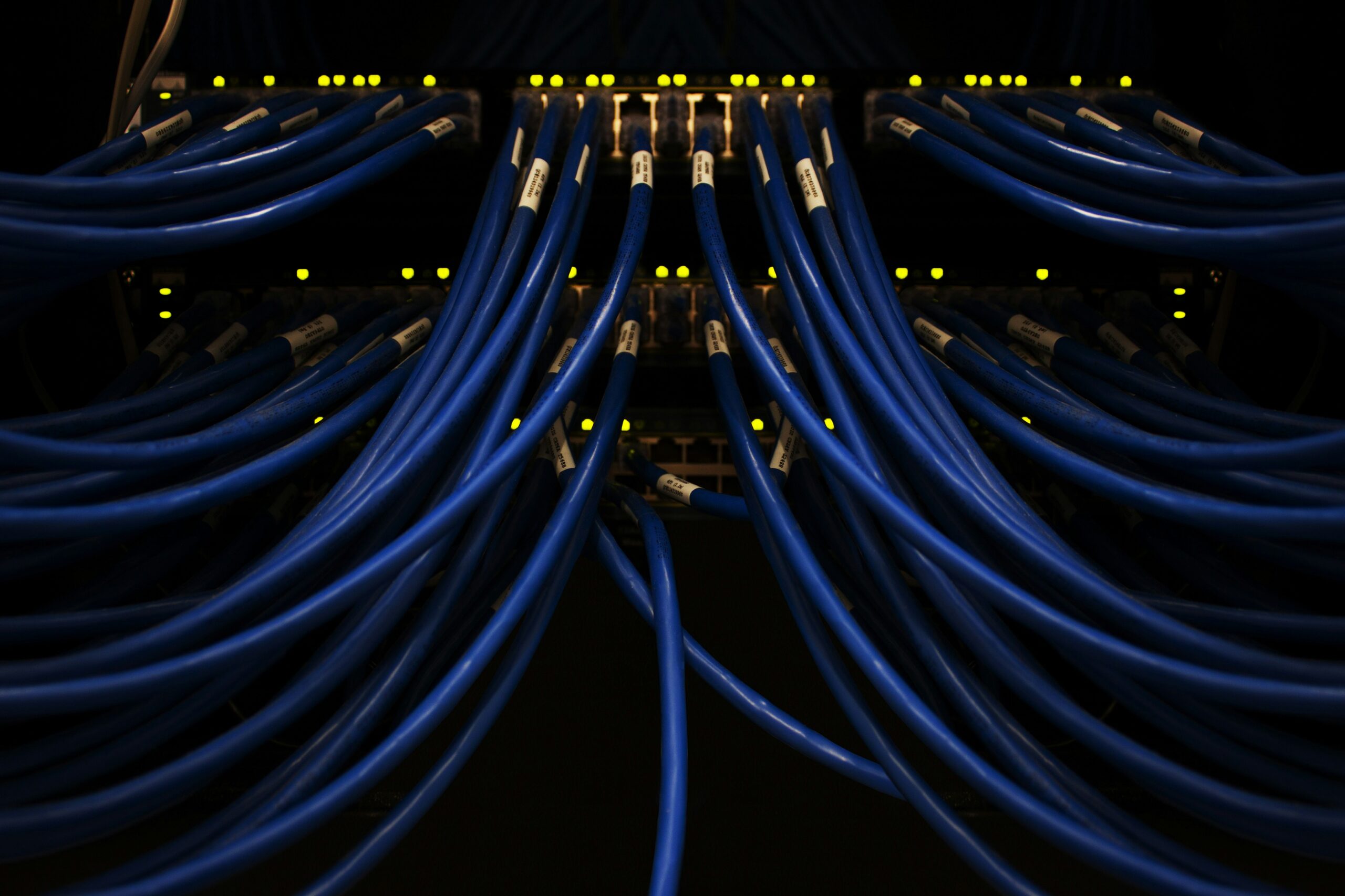
High-Speed Networking & Data Transport
PCBs for enterprise routers, carrier-grade switches, data-center interconnect devices, and multi-gigabit backbone equipment.

Customer Premises & Edge Devices
Electronics for gateways, modems, access points, and edge networking hardware enabling reliable last-mile connectivity.

Cloud & Data Center Networking
High-performance PCBs for switches, servers, and network acceleration hardware supporting scalable cloud infrastructure.

Network Security & Traffic Management Systems
PCBs for firewalls, intrusion detection systems, load balancers, and traffic optimization platforms that require high-throughput processing, low latency, and reliable operation under continuous network load.